You're all caught up—no notifications available.
Explore All Exams at KGS


All Exams
Explore All Exams at KGS

Khan Sir Courses
Geography I Polity I History | World Map I Indian Map I Economics I Biology

UPSC & State PSC
UPSC I BPSC I UP-PSC I MP-PSC

State Exams
UP I Bihar I MP | Rajasthan

NEET | JEE | CUET
NEET | JEE | CUET

Defence Exams
NDA I CDS I CAPF I AFCAT I SSB I Agniveer

Police Exams
UP SI | Bihar SI | Delhi Police | UP Constable

SSC Exams
CGL I CPO I CHSL I MTS I SSC GD I Delhi Police

Foundation Courses
Physics I Chemistry I Biology I History I Geography I Polity I NCERT I Math I English | Map I Reasoning

Railway Exams
RRB | RPF

Teaching Exams
TET | Teaching | UGC

Banking Exams
SBI | RBI | IBPS

Engineering Exams
Civil | Electrical | Mechanical
UGC NET
UGC NET/JRF
Current Affairs provides you with the best compilation of the Daily Current Affairs taking place across the globe: National, International, Sports, Science and Technology, Banking, Economy, Agreement, Appointments, Ranks, and Report and General Studies

SYLLABUS
GS-3: Achievements of Indians in science & technology; indigenization of technology and developing new technology; Awareness in the fields of IT.
Context: NITI Aayog has released India’s first comprehensive 10-year roadmap, " Future of India’s Semiconductor Industry”, aimed at building a USD 120–150 billion semiconductor value chain by 2035 and positioning India as an indispensable player in the global semiconductor ecosystem.
Key Highlights of the Roadmap
• Why India Must Act Now:
o Nearly 90–95% of India's semiconductor demand is met through imports.
o Dependence on imported chips poses strategic risks to defence, aerospace and critical infrastructure systems.
o India spent nearly USD 150 billion on semiconductor imports during FY17–FY25, resulting in significant foreign exchange outflows.
o Domestic semiconductor production is essential for making future technologies such as 5G/6G devices more affordable and accessible.
o Global supply-chain diversification and the China-plus-One strategy have created a narrow but critical window of opportunity for India to enter the semiconductor value chain.
• India's Semiconductor Opportunity:
o The global semiconductor market is expected to exceed USD 1.5 trillion by 2035.
o India's semiconductor demand is projected to reach around USD 200 billion by 2035.
o At present, nearly 90–95% of India's semiconductor demand is met through imports.
o Global supply-chain realignments and the search for trusted manufacturing destinations provide India with a historic opportunity to strengthen its position in the value chain.
• Vision 2035: Becoming Indispensable, Not Imitative
o India aims to capture 10–13% of the global semiconductor market by 2035.
o The roadmap seeks to retain 55–70% of semiconductor value capture within India through local design, packaging, materials and manufacturing ecosystems.
o The roadmap targets the creation of a USD 120–150 billion semiconductor value chain by 2035.
o The strategy is based on three pillars:
1. Strategic self-sufficiency.
2. Ecosystem strength.
3. Global indispensability.
o The emphasis is on building leadership in areas where India possesses structural advantages rather than competing directly in every segment of the semiconductor industry.
o India aims to achieve 15–25% chip self-sufficiency by 2030.
o Self-sufficiency is expected to increase to 35–50% by 2035.
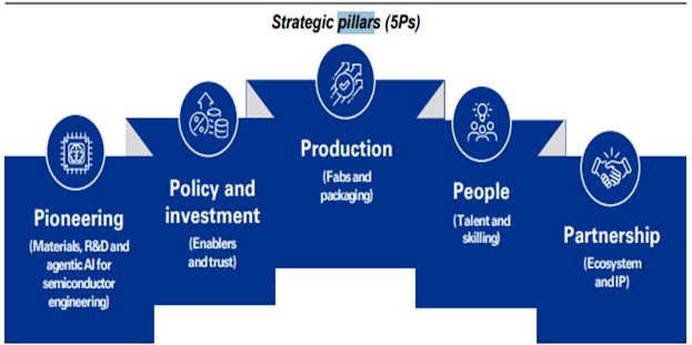
• Leadership in Advanced Packaging and OSAT:
o India aims to emerge as one of the top three global destinations for advanced packaging and OSAT (Outsourced Semiconductor Assembly and Testing).
o Focus areas include Chiplets, 2.5D and 3D integration, Fan-Out Wafer Level Packaging (FOWLP), Panel-Level Packaging (PLP) and System-in-Package (SiP) technologies.
o Advanced packaging is identified as a major opportunity in the emerging "More-than-Moore" era.
• Focus on Compound and Wide-Bandgap Semiconductors:
o The roadmap prioritises leadership in Silicon Carbide (SiC) and Gallium Nitride (GaN) technologies.
o India aims to become a major supplier of wide-bandgap semiconductor materials.
o These technologies are critical for electric vehicles, renewable energy systems, power electronics, telecom infrastructure and defence applications.
• Strengthening Semiconductor Design Capabilities:
o Tiered subsidies for Electronic Design Automation (EDA) tools are proposed to reduce design costs and improve access for startups and researchers.
o An AI-enabled Semiconductor Engineering Mission is proposed to shorten chip-design cycles through agentic AI tools and automation.
o The roadmap targets the creation of more than 100 advanced semiconductor design IPs by 2035.
o Priority areas include AI-native chip design, high-performance computing, quantum computing, system architecture and chiplet-based design.
o The objective is to move from a design-services hub to a creator of globally competitive semiconductor IP.
• Building Domestic Manufacturing Capacity:
o Wafer fabrication efforts will primarily focus on mature logic nodes between 28 nm and 65 nm.
o Special emphasis is placed on analog, mixed-signal and power-management chips used in automotive, IoT and industrial applications.
o The roadmap recommends exploring Small Modular Reactors (SMRs) to provide reliable dedicated power for semiconductor fabrication clusters.
• Alignment with India Semiconductor Mission (ISM) 2.0:
o The roadmap complements the objectives of India Semiconductor Mission (ISM) 2.0 announced in Union Budget 2026.
o It marks India's transition from ecosystem creation to ecosystem deepening.
o Greater emphasis is placed on design, manufacturing, packaging, materials, talent development, research and innovation and global partnerships.
• Major Challenges Identified:
o Rising technological complexity is making semiconductor design and manufacturing increasingly difficult.
o India faces shortages of specialised talent required for fabrication, packaging and advanced research.
o Semiconductor manufacturing requires high capital investments, energy resources and water availability.
o Building trust and acceptance for India-made chips within global supply chains will require sustained efforts.
o Long gestation periods and slow returns increase the financial risks associated with semiconductor investments.
• Roadmap’s Key Solutions:
o Establish a National Frontier Semiconductor Research Programme to accelerate frontier semiconductor R&D.
o Create a National Design and Packaging Co-Design Platform to strengthen indigenous design capabilities.
o Develop a National Fab Academy to build a semiconductor-ready workforce.
o Establish a National Semiconductor Capital Framework to mobilise long-term investments.
o Build sovereign capabilities in semiconductor design, research and advanced packaging.
o Develop a robust domestic manufacturing ecosystem focused on strategic and high-value segments.
o Create a complete semiconductor talent pyramid from technicians to solution architects.
o Mobilise long-term capital through government support and private-sector participation.
o Strengthen trusted international partnerships to accelerate technology acquisition and ecosystem growth.
Sources :
PIB
The Hindu
Niti
Fortune India

NITI Aayog Releases India’s First Semiconductor Roadmap
Supreme Court Issues Comprehensive Guidelines for Curbing Human Trafficking
Skycast Aviation Weather Monitoring System
Supreme Court Issues Comprehensive Guidelines for Curbing Human Trafficking
Skycast Aviation Weather Monitoring System
India’s First Hydrogen-Powered Train
Insolvency and Bankruptcy Code (IBC) – 10 Years
Cabinet Approves SARTHAK-PDS Scheme to Modernise Public Distribution System
The most trusted learning platform on your phone
With our training programs, learning online can be a very exciting experience! Take the next step toward achieving your professional and personal objectives



Course Related Query:
Ask Your DoubtsStore Related Query:[email protected]NCERT Books
Resources
We love learning. Through our innovative solutions, we encourage ourselves, our teams, and our Students to grow. We welcome and look for diverse perspectives and opinions because they enhance our decisions. We strive to understand the big picture and how we contribute to the company’s objectives. We approach challenges with optimism and harness the power of teamwork to accomplish our goals. These aren’t just pretty words to post on the office wall. This is who we are. It’s how we work. And it’s how we approach every interaction with each other and our Students.
Come with an open mind, hungry to learn, and you’ll experience unmatched personal and professional growth, a world of different backgrounds and perspectives, and the freedom to be you—every day. We strive to build and sustain diverse teams and foster a culture of belonging. Creating an inclusive environment where every students feels welcome, appreciated, and heard gives us something to feel (really) good about.
Get Free academic Counseling & Course Details